Custom ASICs for Real-Time Inference at the Edge
Uncategorized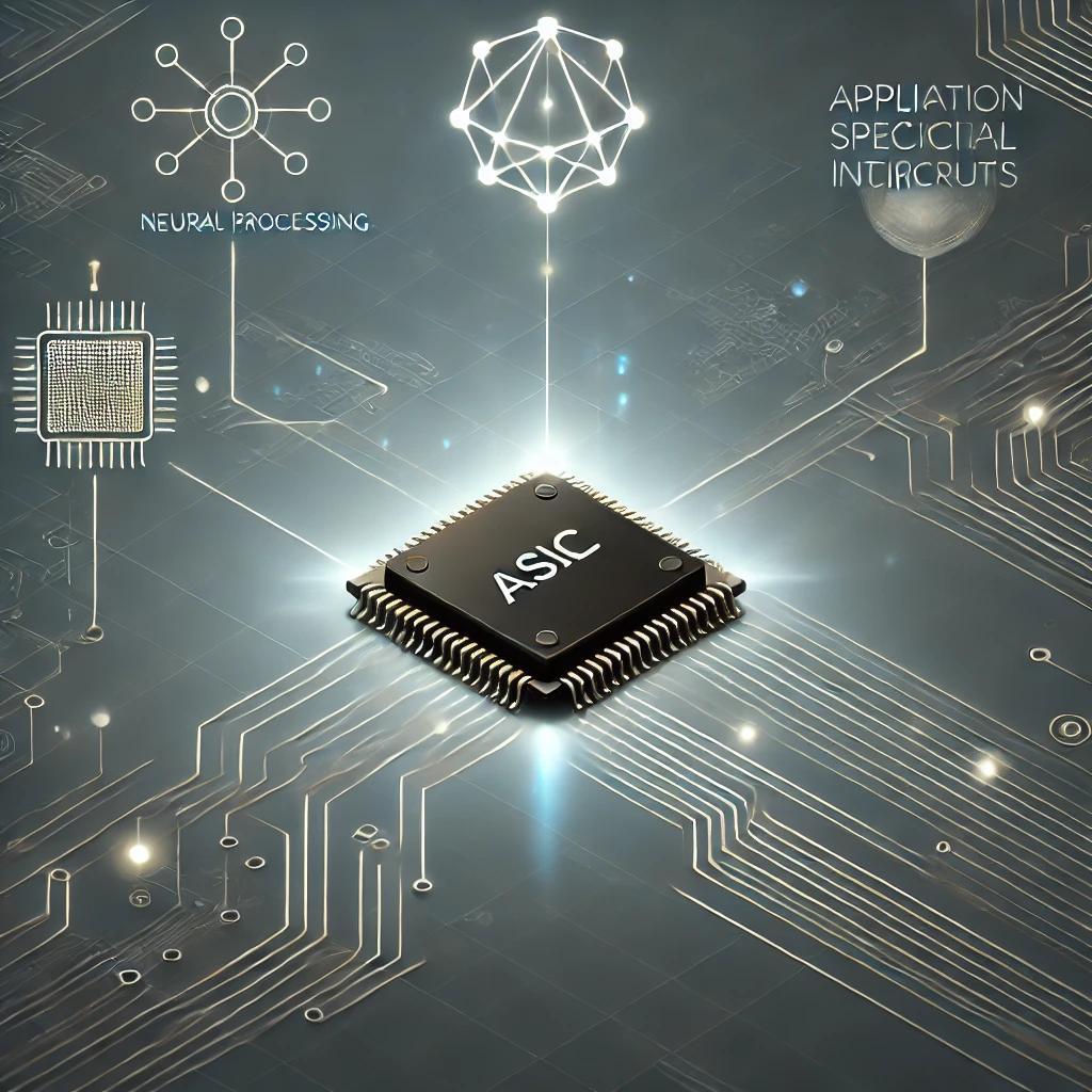
Introduction
Edge computing is revolutionizing how we process and interact with data by enabling real-time AI-powered decision-making directly on local devices. This paradigm shift removes the dependency on cloud infrastructure for critical tasks, reducing latency, enhancing privacy, and ensuring reliable operation even in connectivity-challenged environments. However, achieving this level of responsiveness and autonomy requires hardware that is both efficient and tailored to the unique constraints of edge deployment—including limited power, compact form factor, and the need for ultra-low latency.
Traditional processors like CPUs and GPUs, while versatile, are often inefficient for executing deep learning inference at the edge. CPUs lack the parallelism needed for high-speed computation, and GPUs, although powerful, are power-hungry and often too large for embedded systems. This gap has driven the rise of custom Application-Specific Integrated Circuits (ASICs) purpose-built for AI inference.
Custom ASICs are designed to perform specific AI workloads such as convolutional neural network (CNN) inference, image recognition, or sensor data analysis with exceptional efficiency. By hardwiring only the necessary logic and data paths, these chips dramatically reduce power consumption, minimize thermal output, and allow for miniaturization without compromising performance.
In this article, we explore the architecture and design trade-offs of AI-focused ASICs, including fixed-function vs. programmable logic, memory hierarchy optimization, and dataflow architectures like systolic arrays. We also examine real-world deployments across autonomous vehicles, smart cameras, industrial IoT, and medical wearables—where custom ASICs are delivering fast, reliable AI at the edge. As edge AI continues to scale across industries, custom ASICs will be critical enablers—pushing the boundaries of what’s possible in smart, decentralized computing.
What Are Custom ASICs?
An Application-Specific Integrated Circuit (ASIC) is a type of microchip designed for a specific application rather than general-purpose use. Unlike general-purpose processors, custom ASICs are optimized at the hardware level for specific computational tasks, making them ideal for targeted performance in edge AI environments.
Types of ASICs for AI:
- Fixed-function ASICs: Designed to execute specific tasks like convolution operations or activation functions.
- Configurable ASICs: Include limited reprogrammability to adapt to different models or parameters.
- Neuromorphic ASICs: Mimic brain-like structures for spiking neural networks and ultra-low-power AI.
Why Edge AI Needs Custom ASICs
Edge AI refers to deploying machine learning models on devices at the edge of the network—like smartphones, drones, cameras, wearables, and industrial sensors. These deployments pose several unique challenges:
- Power Efficiency: Many edge devices run on batteries and need ultra-low-power processing.
- Latency Sensitivity: Real-time decision-making (e.g., for autonomous vehicles or medical monitoring) requires sub-millisecond inference times.
- Thermal Constraints: Passive cooling or compact enclosures necessitate low thermal footprints.
- Connectivity Limitations: Devices cannot always rely on cloud-based inference due to bandwidth or security constraints.
- Security and Privacy: Processing data locally enhances privacy and reduces exposure.
Custom ASICs excel in all these areas by tailoring the hardware to the exact needs of the inference task, eliminating inefficiencies present in general-purpose architectures.
Key Architectural Features of Edge Inference ASICs
Designing a custom ASIC for AI inference involves several architectural strategies to ensure optimal performance at the edge:
1. Dataflow Architecture
Dataflow architectures emphasize parallel and pipeline processing, enabling efficient computation with minimal memory access. This reduces latency and power consumption.
2. On-Chip Memory Hierarchy
Edge ASICs integrate specialized SRAM blocks and cache hierarchies to store weights and activations, minimizing energy-expensive off-chip memory access.
3. Quantization and Low-Precision Arithmetic
AI inference at the edge often uses quantized models (e.g., INT8, INT4), and ASICs are designed to handle these efficiently. Custom ALUs can process low-precision arithmetic faster and with lower power draw.
4. Weight Sparsity Exploitation
Many AI models have sparse weight matrices. ASICs can skip zero-value computations, reducing energy consumption and computation time.
5. Custom Accelerators for AI Primitives
ASICs include hardwired blocks for:
- Convolution
- Matrix multiplication
- Activation functions
- Batch normalization
- Pooling operations
6. Edge-Centric IO and Interconnects
Custom ASICs are equipped with interfaces for common edge sensors, cameras, or radio modules (e.g., MIPI, SPI, I2C), making them plug-and-play in embedded systems.
Design Considerations for Edge AI ASICs
Developing a custom ASIC involves a balance of multiple engineering priorities:
1. Model Compatibility
The ASIC must support the AI models used in the target application. This often requires tailoring the chip’s data paths and memory sizes to the model’s layer structure.
2. Silicon Area and Cost
Since ASICs are fabricated for specific use cases, designers aim to minimize die size and production cost while maximizing performance.
3. Thermal Design Power (TDP)
ASICs are often passively cooled, so their thermal profiles must remain within strict limits.
4. Lifecycle and Updatability
Unlike software, hardware cannot be easily updated post-fabrication. Some designs include limited configurability or soft-programmable logic blocks.
5. Security Features
Custom AI ASICs may incorporate features like encrypted boot, secure enclaves, and model protection to prevent reverse engineering or tampering.
Tools and Methodologies
Creating a custom ASIC involves specialized tools and workflows:
- High-Level Synthesis (HLS): Converts algorithms written in C/C++ or Python into hardware descriptions.
- Hardware Description Languages (HDLs): Such as Verilog or VHDL, used to define chip logic.
- AI Model Profiling: Tools like TensorRT or TVM are used to profile models for identifying hardware bottlenecks.
- ASIC Design Suites: Tools like Cadence, Synopsys, or Mentor Graphics for layout, simulation, and fabrication.
- FPGA Prototyping: Before final fabrication, many designs are tested on FPGAs to validate performance.
Real-World Applications
Custom ASICs are already making an impact across industries:
1. Smartphones and Wearables
Chips like Apple’s Neural Engine and Google’s Edge TPU enable real-time photo enhancement, face recognition, and voice processing on-device.
2. Smart Cameras and Surveillance
ASICs process video streams in real time for object detection, facial recognition, and behavior analysis—without sending data to the cloud.
3. Autonomous Vehicles
Companies like Tesla and Mobileye develop in-house AI ASICs for perception, planning, and control, reducing latency and enhancing safety.
4. Healthcare Devices
Wearable health monitors use AI ASICs for real-time ECG analysis, fall detection, and anomaly detection.
5. Industrial IoT
Smart factories and robotics use ASICs for visual inspection, predictive maintenance, and sensor fusion.
Key Players in Custom Edge AI ASICs
Several companies are pioneering the development of edge AI ASICs:
- Google – Edge TPU
- Apple – Neural Engine
- NVIDIA – Jetson SoCs with dedicated inference cores
- Intel – Movidius VPU
- Qualcomm – AI Engine on Snapdragon
- Mythic AI – Analog compute-in-memory ASICs
- Tenstorrent – Reconfigurable AI accelerators
Benefits of Custom ASICs for Edge Inference
1. Ultra-Low Latency
Custom ASICs deliver near-instantaneous inference, crucial for latency-sensitive applications such as augmented reality (AR), virtual reality (VR), and autonomous navigation. These environments demand split-second decision-making, and ASICs eliminate the delay caused by offloading computations to remote servers, ensuring seamless performance and real-time interaction in mission-critical scenarios.
2. Minimal Power Consumption
Designed specifically for targeted AI tasks, custom ASICs operate with extreme energy efficiency. They consume significantly less power than general-purpose processors, enabling battery-powered edge devices like drones, wearables, and sensors to run complex AI models for longer periods without sacrificing performance or requiring frequent recharging or bulky cooling systems.
3. Smaller Footprint
Custom ASICs are compact and optimized for integration into space-constrained environments. Their small physical footprint makes them ideal for embedded systems in applications such as medical implants, industrial automation, and portable devices, where real estate is limited and performance cannot be compromised despite the device’s miniature form factor.
4. Increased Privacy
By processing data locally on the device, ASICs help minimize the need to transmit sensitive information to the cloud. This local processing enhances user privacy, reduces exposure to cyber threats, and simplifies compliance with data protection regulations like GDPR, especially in healthcare, finance, and surveillance applications.
5. Optimized Cost per Inference
In high-volume, single-purpose applications, custom ASICs reduce the cost per inference by eliminating unnecessary computation and maximizing throughput. Their streamlined architecture is perfect for repetitive tasks such as facial recognition, quality inspection, or voice activation, making them a cost-effective solution for scaling AI across large deployments.
Limitations and Challenges
1. High Upfront Costs
Designing and fabricating custom ASICs requires substantial investment in engineering, tooling, and manufacturing. These high non-recurring engineering (NRE) costs make ASICs financially viable primarily for large-scale deployments. Small companies or niche applications may struggle to justify the initial capital required, despite potential long-term gains in performance and efficiency.
2. Inflexibility
Fixed-function ASICs are hardwired for specific tasks, offering little to no flexibility after deployment. Once manufactured, they cannot be updated to accommodate new algorithms, model architectures, or changing standards. This rigidity can limit longevity and adaptability, especially in fast-moving fields like AI where models evolve rapidly.
3. Long Design Cycles
Developing an ASIC involves multiple complex stages—specification, simulation, physical design, fabrication, and validation. This process often takes several months, delaying time-to-market. Iterations due to design bugs or performance issues can extend this timeline further, making ASICs less suitable for projects requiring rapid development or frequent updates.
4. Dependency on Accurate Forecasts
ASICs are typically produced in large batches, meaning accurate forecasting of market demand is essential. Overestimating can result in surplus inventory and financial loss, while underestimating can lead to shortages and missed opportunities. The inability to easily scale production adds risk to the investment in ASIC development.
5. Limited Vendor Ecosystem
Unlike CPUs or GPUs, the ASIC development ecosystem is more specialized and less mature. There are fewer toolchains, IP libraries, and foundries catering to custom AI ASICs. This scarcity can lead to higher costs, limited design flexibility, and increased reliance on niche vendors for development and support.
The Future of Edge AI ASICs
1. AI Model Co-Design
Future AI models will be developed with hardware constraints in mind, ensuring optimal alignment with ASIC architecture. This tight co-design approach enhances performance and energy efficiency by minimizing unnecessary computations, memory bottlenecks, and latency—enabling more effective deployment of complex models on resource-constrained edge devices.
2. Heterogeneous Integration
Advanced packaging techniques will enable ASICs to be integrated alongside FPGAs, CPUs, or analog processors in a single chiplet-based system. This heterogeneous architecture allows for task-specific acceleration, combining the strengths of each processing unit to handle diverse workloads more efficiently while maintaining low latency and power consumption at the edge.
3. Analog and In-Memory Computing
Emerging paradigms like compute-in-memory and analog processing reduce the need to move data between memory and compute units—cutting power usage and increasing speed. These approaches, when paired with ASICs, can dramatically enhance energy efficiency, especially for inference tasks in always-on devices like wearables or remote sensors.
4. AutoML and Hardware-Aware Training
Automated Machine Learning (AutoML) tools will increasingly design neural networks tailored to specific ASIC configurations. These hardware-aware techniques optimize model architectures for memory access patterns, computation precision, and core utilization—ensuring models are not only accurate but also highly efficient on their intended silicon.
5. Open-Source ASICs
Initiatives like OpenROAD and the Skywater PDK are lowering the barriers to custom chip design by offering free tools and open fabrication resources. This democratization enables startups, researchers, and smaller companies to build ASICs tailored to their AI applications, fostering innovation and expanding access to high-performance edge AI.
Conclusion
Custom ASICs are rapidly emerging as the cornerstone of real-time AI inference at the edge, offering a potent combination of ultra-low latency, high energy efficiency, and task-specific acceleration. Unlike general-purpose CPUs and GPUs, which must accommodate a wide range of computing tasks, ASICs are purpose-built to execute specific AI models with unparalleled speed and efficiency. This specialization enables edge devices to process complex neural networks locally—without relying on cloud connectivity—making them ideal for time-sensitive applications like autonomous vehicles, augmented reality (AR), medical diagnostics, and smart surveillance.
As AI continues to expand into all facets of life—from wearable health monitors and industrial automation to intelligent home appliances and smart infrastructure—the role of custom ASICs becomes even more vital. These chips empower devices to interpret, analyze, and act on data in real time, reducing latency and enhancing user experiences while maintaining data privacy by keeping inference on-device.
Furthermore, innovations in AI model compression, quantization, and hardware-aware training are making it easier to deploy powerful models on compact silicon. Coupled with open-source ASIC design tools and collaborative platforms, the barriers to entry are lowering, enabling broader innovation. In the coming years, custom ASICs will be central to scaling AI seamlessly and securely at the edge.