3D Integrated Circuits for AI Hardware Scaling
Uncategorized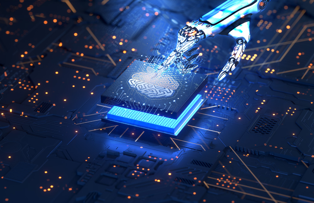
Introduction
As artificial intelligence (AI) models continue to scale in complexity—driven by advancements in deep learning, natural language processing, and generative AI—the underlying hardware must evolve to meet ever-growing demands for computational power, memory access, and energy efficiency. Traditional 2D chip architectures, with their planar layouts and limited interconnect capabilities, are increasingly hitting performance bottlenecks in terms of latency, data transfer, and heat dissipation. This has paved the way for 3D Integrated Circuits (3D ICs)—a groundbreaking approach to chip design that stacks multiple layers of active silicon dies vertically.
3D ICs provide a radical departure from conventional chip designs by enabling components such as processors, memory, and interconnects to be integrated in tightly packed vertical layers. This vertical stacking reduces the physical distance between compute and memory units, dramatically increasing memory bandwidth while lowering latency and power consumption. For AI workloads, which require frequent and large data transfers between layers of memory and compute units, these benefits are crucial.
Beyond performance, 3D ICs also offer improved scalability. As AI models grow from millions to billions of parameters, 3D architectures make it possible to fit more transistors and memory cells in a compact footprint, overcoming the limitations of Moore’s Law. Moreover, they open up new possibilities for heterogeneous integration, where AI accelerators, logic, and memory chips fabricated with different technologies can be stacked and interconnected seamlessly.
However, 3D ICs also introduce new challenges, such as thermal management, complex fabrication processes, and reliability concerns at scale. Despite these hurdles, major tech companies and research institutions are actively investing in 3D IC development, signaling its critical role in the future of AI hardware. In sum, 3D ICs represent a pivotal advancement in the ongoing effort to sustain and accelerate AI innovation through smarter, denser, and more efficient hardware architectures.
What Are 3D Integrated Circuits?
3D Integrated Circuits are semiconductor devices built by stacking multiple layers of active electronic components vertically into a single chip. These layers are connected using advanced interconnect technologies such as Through-Silicon Vias (TSVs) or micro-bumps, enabling ultra-fast communication between stacked layers.
Types of 3D Integration:
- Monolithic 3D ICs: Layers are fabricated sequentially on a single wafer.
- TSV-Based 3D ICs: Separate dies are stacked and connected using TSVs.
- 2.5D Integration: Uses an interposer to connect multiple dies side-by-side, offering a balance between performance and cost.
Why AI Needs 3D ICs
AI workloads, especially in deep learning, are incredibly data- and compute-intensive. Traditional 2D architectures face several limitations:
- Memory Bottleneck: The Von Neumann architecture separates memory and compute, leading to data transfer delays.
- Latency and Bandwidth: Off-chip memory access is slow and energy-inefficient.
- Power Dissipation: More data movement means more heat, impacting performance.
- Scalability Limits: Moore’s Law is slowing, making vertical scaling more attractive.
3D ICs address these issues by bringing memory closer to compute, reducing the distance data needs to travel, increasing bandwidth, and improving energy efficiency—making them ideal for AI hardware.
Architectural Advantages of 3D ICs for AI
1. Increased Memory Bandwidth
With memory stacks sitting directly above compute layers, 3D ICs offer significantly higher bandwidth. High Bandwidth Memory (HBM) technologies, for example, are widely used in AI accelerators.
2. Reduced Latency
Shorter interconnects between memory and processors dramatically reduce latency, which is critical for real-time AI inference and training.
3. Lower Power Consumption
3D ICs consume less power due to shorter wiring and reduced I/O energy. This is especially beneficial in edge AI applications.
4. Smaller Footprint
By stacking components vertically, 3D ICs allow for denser integration, reducing chip size while increasing performance.
5. Heterogeneous Integration
3D ICs can integrate diverse components—CPUs, GPUs, memory, and AI accelerators—into a single stack for optimized system-on-chip designs.
Key Technologies Behind 3D ICs
1. Through-Silicon Vias (TSVs)
TSVs are vertical electrical connections passing through silicon wafers or dies, enabling communication between stacked layers.
2. Micro-Bumps and Hybrid Bonding
Used to establish inter-die connections. Hybrid bonding provides better electrical and mechanical characteristics compared to micro-bumps.
3. Wafer-to-Wafer and Die-to-Wafer Bonding
These bonding methods determine how layers are stacked—either whole wafers or individual dies.
4. Thermal Management Materials
Advanced heat spreaders, thermal interface materials (TIMs), and microfluidic cooling are used to dissipate heat effectively.
Design Considerations for AI Hardware Using 3D ICs
Designing AI hardware with 3D ICs requires careful planning to balance performance, cost, and thermal constraints:
1. Thermal Challenges
Stacking active layers increases power density, necessitating advanced cooling techniques to prevent thermal throttling.
2. Yield and Manufacturing Complexity
Fabrication of multiple functional layers increases defect probability. A single defect in one layer can render the entire stack unusable.
3. Cost vs. Benefit Trade-offs
3D ICs are more expensive to produce but may reduce system costs through higher integration and performance-per-watt gains.
4. Design Automation Tools
EDA tools for 3D design are still evolving. Tools must support thermal analysis, interconnect planning, and signal integrity in 3D space.
5. Testing and Debugging
Testing 3D ICs is more complex than traditional chips due to limited access to internal layers.
Use Cases and Applications in AI
1. AI Training Accelerators
Training massive neural networks requires huge memory bandwidth and compute. NVIDIA’s GPUs with stacked HBM are a prime example.
2. Edge AI Devices
Devices like smartphones and wearables benefit from smaller, low-power 3D ICs that integrate AI acceleration locally.
3. Data Center AI Infrastructure
3D ICs enable higher compute density in servers, enhancing AI model serving and inferencing at scale.
4. Neuromorphic Computing
Brain-inspired architectures like IBM’s TrueNorth can benefit from vertical integration for mimicking 3D neural structures.
5. Autonomous Vehicles
Real-time processing of sensor data for perception and decision-making requires high-performance, low-latency chips enabled by 3D stacking.
Leading Companies and Research Initiatives
Industry Players:
- Intel: Foveros 3D packaging technology for heterogeneous integration.
- TSMC: Chip-on-wafer-on-substrate (CoWoS) and System-on-Integrated-Chips (SoIC) solutions.
- Samsung: Pioneering HBM and 3D NAND for AI applications.
- AMD: 3D V-Cache technology for stacking cache memory atop CPUs.
Academic and Research Labs:
- MIT: Research on monolithic 3D integration for AI.
- Stanford: Projects focusing on thermal-aware 3D architectures.
- DARPA: Funding 3D integration for defense and AI.
Emerging Trends and Innovations
1. AI-Specific 3D IC Co-Design
Future designs will co-optimize AI models and 3D hardware together, improving hardware utilization and inference speed.
2. Chiplet Architectures
Using chiplets (modular dies) stacked in 3D allows for flexible, scalable AI hardware tailored to specific workloads.
3. Photonic Interconnects
Integrating optical communication layers within 3D stacks to overcome electrical bottlenecks.
4. 3D Memory Hierarchies
Stacked SRAM, DRAM, and non-volatile memories (like ReRAM) create new multi-tiered memory designs ideal for AI data flows.
5. Integration with Analog AI
Combining analog computing elements in 3D stacks for in-memory computing and ultra-low-power AI inference.
Advantages of 3D ICs for AI Scaling
1. Scalable Performance
3D ICs allow vertical stacking of processing and memory layers, enabling designers to add computational power without increasing chip footprint. This scalability is ideal for AI applications, where larger models demand higher performance. As model complexity grows, additional layers can be added to meet performance targets without redesigning the entire chip.
2. Energy Efficiency
By reducing the physical distance between processing and memory units, 3D ICs minimize data movement, which is a major source of power consumption in AI workloads. Shorter interconnects mean lower capacitance and reduced energy per operation, making 3D ICs significantly more power-efficient compared to traditional 2D architectures, especially in edge AI applications.
3. Modularity
3D ICs support heterogeneous integration, allowing different dies—each optimized for specific functions like logic, memory, or AI acceleration—to be stacked together. This modularity improves design flexibility, enabling the creation of custom AI chips tailored to particular workloads while also streamlining upgrades and revisions by replacing only specific layers when needed.
4. Higher Bandwidth
The vertical stacking in 3D ICs provides much shorter and wider data paths between compute and memory layers, enabling significantly higher memory bandwidth. This is particularly advantageous for AI tasks that require rapid access to large datasets or model parameters, leading to faster inference and training speeds with reduced latency.
5. Compact Designs
With multiple layers of logic and memory stacked in a single package, 3D ICs offer greater functionality in a smaller area. This compactness is ideal for space-constrained environments like mobile devices, wearables, or embedded systems, allowing advanced AI capabilities to be embedded directly into consumer electronics and edge devices.
Challenges to Overcome
1. Thermal Management
Stacking multiple active layers in 3D ICs significantly increases power density, making heat dissipation a major challenge. Without effective thermal management strategies—such as advanced cooling systems or thermal-aware floorplanning—overheating can degrade performance, shorten device lifespan, and limit the scalability of AI hardware that relies on sustained high-performance operations.
2. Design Complexity
Designing 3D ICs involves intricate architectural decisions, including inter-layer communication, thermal planning, and signal integrity. It requires sophisticated Electronic Design Automation (EDA) tools and expertise in heterogeneous integration. The added complexity can extend development timelines and increase design costs, making it more demanding than conventional 2D chip design.
3. Yield Issues
Each layer in a 3D IC must meet stringent quality standards, and defects in any die can compromise the entire stack. This leads to lower manufacturing yields compared to 2D ICs, driving up production costs and limiting scalability. Improving fabrication processes and defect tolerance is essential to mitigate this issue.
4. Standardization
Currently, there’s a lack of universal standards for interconnects, packaging, and testing in 3D ICs. This hampers interoperability across vendors and toolchains, making ecosystem development difficult. Standardized protocols and interfaces are crucial for accelerating adoption and enabling smoother integration into diverse AI hardware platforms.
5. Economic Viability
While 3D ICs offer performance and efficiency gains, they come at a high development and manufacturing cost. For widespread adoption, the performance benefits must clearly outweigh the economic investment. Achieving this balance requires mature fabrication processes, optimized architectures, and broader market demand to drive economies of scale.
Future Outlook
3D ICs represent the future of AI hardware scaling, offering a path forward as traditional scaling slows. Over the next decade, we can expect:
- Widespread adoption of chiplets and stacked AI accelerators
- Enhanced co-design methodologies involving AI frameworks and hardware architectures
- Proliferation of 3D ICs in edge and wearable devices
- Breakthroughs in cooling technologies for vertical stacks
- Integration with quantum and neuromorphic systems
Conclusion
3D Integrated Circuits (3D ICs) represent a transformative leap in semiconductor technology, particularly in the context of artificial intelligence (AI) and high-performance computing. Unlike traditional 2D chips, which lay out transistors and components on a single plane, 3D ICs vertically stack multiple layers of logic and memory, interconnected through high-speed vertical vias such as Through-Silicon Vias (TSVs). This vertical integration fundamentally changes how data is processed and moved across a chip, enabling unprecedented performance gains.
The demand for AI accelerators has grown rapidly, driven by the proliferation of complex models like large language models (LLMs), generative AI, and real-time inference engines. These models require immense computational power, high memory bandwidth, and energy-efficient data transfer—challenges that conventional chip designs are struggling to meet. 3D ICs address these issues head-on by drastically reducing the physical distance between memory and compute units, thereby minimizing latency and power consumption while increasing bandwidth. This close integration is especially advantageous for AI workloads, which are often memory-bound and require rapid access to vast amounts of data.
Moreover, 3D ICs support a modular design approach. Different dies within a 3D stack can be optimized for specialized tasks—such as processing, memory, I/O, or even analog computing—enabling heterogeneous integration that maximizes system performance and efficiency. This modularity also opens the door for rapid innovation, allowing manufacturers to upgrade specific layers without redesigning the entire chip.
However, the shift to 3D integration is not without challenges. Issues like thermal management, yield optimization, and standardization must be addressed to ensure reliable and scalable production. Fortunately, advances in materials science, chiplet architectures, and electronic design automation (EDA) tools are beginning to alleviate these concerns, making 3D ICs more viable for widespread deployment. As AI continues to permeate sectors such as autonomous vehicles, healthcare, finance, and smart cities, the importance of scalable, high-performance, and power-efficient hardware will only grow. 3D ICs offer a compelling solution, enabling the next wave of intelligent computing systems.